- 您现在的位置:买卖IC网 > Sheet目录3878 > PIC18F23K20-I/SP (Microchip Technology)IC PIC MCU FLASH 4KX16 28-DIP
2009 Microchip Technology Inc.
Advance Information
DS41297F-page 15
PIC18F2XK20/4XK20
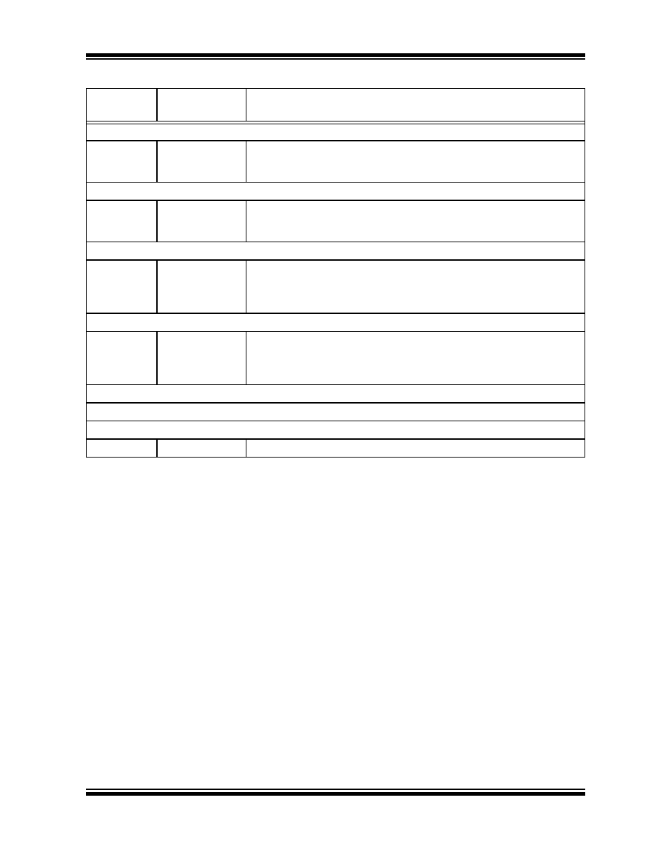
TABLE 3-3:
ERASE CODE MEMORY CODE SEQUENCE
4-bit
Command
Data Payload
Core Instruction
Step 1: Direct access to code memory and enable writes.
0000
8E A6
9C A6
84 A6
BSF
EECON1, EEPGD
BCF
EECON1, CFGS
BSF
EECON1, WREN
Step 2: Point to first row in code memory.
0000
6A F8
6A F7
6A F6
CLRF
TBLPTRU
CLRF
TBLPTRH
CLRF
TBLPTRL
Step 3: Enable erase and erase single row.
0000
88 A6
82 A6
00 00
BSF
EECON1, FREE
BSF
EECON1, WR
NOP
Erase starts on the 4th clock of this instruction
Step 4: Poll WR bit. Repeat until bit is clear.
0000
0010
50 A6
6E F5
00 00
<MSB><LSB>
MOVF EECON1, W, 0
MOVWF TABLAT
NOP
Shift out data(1)
Step 5: Hold PGC low for time P10.
Step 6: Repeat step 3 with Address Pointer incremented by 64 until all rows are erased.
Step 7: Disable writes.
0000
94 A6
BCF EECON1, WREN
Note 1:
See Figure 4-4 for details on shift out data timing.
发布紧急采购,3分钟左右您将得到回复。
相关PDF资料
PIC18F2515-E/SO
IC MCU FLASH 24KX16 28SOIC
PIC24F08KL401-I/MQ
IC MCU 16BIT 8KB FLASH 20-QFN
PIC16C55A-04/SP
IC MCU OTP 512X12 28DIP
PIC18F2431T-I/ML
IC MCU FLASH 8KX16 28QFN
PIC16LF1938-I/SO
IC MCU 8BIT FLASH 28SOIC
PIC16F639-E/SO
IC MCU FLASH 2KX14 20SOIC
PIC24F08KL402-I/SS
IC MCU 16BIT 8KB FLASH 28-SSOP
PIC16F1936-I/MV
IC MCU 8BIT 14KB FLASH 28UQFN
相关代理商/技术参数
PIC18F23K20-I/SS
功能描述:8位微控制器 -MCU 8 KB Enh Flash 768 RAM 25 I/O Pb Free RoHS:否 制造商:Silicon Labs 核心:8051 处理器系列:C8051F39x 数据总线宽度:8 bit 最大时钟频率:50 MHz 程序存储器大小:16 KB 数据 RAM 大小:1 KB 片上 ADC:Yes 工作电源电压:1.8 V to 3.6 V 工作温度范围:- 40 C to + 105 C 封装 / 箱体:QFN-20 安装风格:SMD/SMT
PIC18F23K20T-I/ML
功能描述:8位微控制器 -MCU 8 KB Enh Flash 768 RAM 25 I/O Pb Free RoHS:否 制造商:Silicon Labs 核心:8051 处理器系列:C8051F39x 数据总线宽度:8 bit 最大时钟频率:50 MHz 程序存储器大小:16 KB 数据 RAM 大小:1 KB 片上 ADC:Yes 工作电源电压:1.8 V to 3.6 V 工作温度范围:- 40 C to + 105 C 封装 / 箱体:QFN-20 安装风格:SMD/SMT
PIC18F23K20T-I/MV
功能描述:8位微控制器 -MCU 8KB Flash 768B RAM Enhanced Flash RoHS:否 制造商:Silicon Labs 核心:8051 处理器系列:C8051F39x 数据总线宽度:8 bit 最大时钟频率:50 MHz 程序存储器大小:16 KB 数据 RAM 大小:1 KB 片上 ADC:Yes 工作电源电压:1.8 V to 3.6 V 工作温度范围:- 40 C to + 105 C 封装 / 箱体:QFN-20 安装风格:SMD/SMT
PIC18F23K20T-I/SO
功能描述:8位微控制器 -MCU 8 KB Enh Flash 768 RAM 25 I/O Pb Free RoHS:否 制造商:Silicon Labs 核心:8051 处理器系列:C8051F39x 数据总线宽度:8 bit 最大时钟频率:50 MHz 程序存储器大小:16 KB 数据 RAM 大小:1 KB 片上 ADC:Yes 工作电源电压:1.8 V to 3.6 V 工作温度范围:- 40 C to + 105 C 封装 / 箱体:QFN-20 安装风格:SMD/SMT
PIC18F23K20T-I/SS
功能描述:8位微控制器 -MCU 8 KB Enh Flash 768 RAM 25 I/O Pb Free RoHS:否 制造商:Silicon Labs 核心:8051 处理器系列:C8051F39x 数据总线宽度:8 bit 最大时钟频率:50 MHz 程序存储器大小:16 KB 数据 RAM 大小:1 KB 片上 ADC:Yes 工作电源电压:1.8 V to 3.6 V 工作温度范围:- 40 C to + 105 C 封装 / 箱体:QFN-20 安装风格:SMD/SMT
PIC18F23K22-E/ML
功能描述:8位微控制器 -MCU 8KB Flash 768b RAM SERIAL EE IND RoHS:否 制造商:Silicon Labs 核心:8051 处理器系列:C8051F39x 数据总线宽度:8 bit 最大时钟频率:50 MHz 程序存储器大小:16 KB 数据 RAM 大小:1 KB 片上 ADC:Yes 工作电源电压:1.8 V to 3.6 V 工作温度范围:- 40 C to + 105 C 封装 / 箱体:QFN-20 安装风格:SMD/SMT
PIC18F23K22-E/MV
功能描述:8位微控制器 -MCU 8KB Flash 768b RAM SERIAL EE IND RoHS:否 制造商:Silicon Labs 核心:8051 处理器系列:C8051F39x 数据总线宽度:8 bit 最大时钟频率:50 MHz 程序存储器大小:16 KB 数据 RAM 大小:1 KB 片上 ADC:Yes 工作电源电压:1.8 V to 3.6 V 工作温度范围:- 40 C to + 105 C 封装 / 箱体:QFN-20 安装风格:SMD/SMT
PIC18F23K22-E/SO
功能描述:8位微控制器 -MCU 8KB Flash 768b RAM SERIAL EE IND RoHS:否 制造商:Silicon Labs 核心:8051 处理器系列:C8051F39x 数据总线宽度:8 bit 最大时钟频率:50 MHz 程序存储器大小:16 KB 数据 RAM 大小:1 KB 片上 ADC:Yes 工作电源电压:1.8 V to 3.6 V 工作温度范围:- 40 C to + 105 C 封装 / 箱体:QFN-20 安装风格:SMD/SMT